
Jensen's Inequality - On AI Chips
Generalist or Specialist in AI Computing?


TLDR: This article is about chips and computing in the AI space. It is designed to provide some context for a semi-technical audience for how the space might evolve and some of the relevant factors. Below is a table of contents to skip to different sections.
Contents:
Stargate
There are rumors that OpenAI intends to raise $100B+ in the near future. That's a capital raise, not a valuation. Microsoft has already put its hat in the ring to build a $100B data center called "Stargate"1. Data centers are being planned in the multi-gigawatt production range with a gigawatt roughly equivalent to the power required for 1M homes or the output of a nuclear reactor of moderate size2.
These numbers sound extraordinary -- and they are. In any situation where there are eye-watering projections (and these are indeed eye-watering especially when considering that private companies are speaking about building nation-scale infrastructure), I find it useful to think about trajectories. There has not historically been a time where exponentials have persisted -- we may be in the middle of such a black swan, but it would be unique in history. Central to this is the nature of computing in the era of AI. This article is intended to provide a bit of intuition about the mechanism of AI computing and some context to the headlines. Like always, it will be semi-technical, and additional information will be referenced throughout for more interested readers.
When Did "Compute" Become a Noun?
It has always been an oddity to me that the field has adopted a verb as its primary noun. To me, it represents a more general blanketing of terms around AI that might be helpful to elucidate a bit before we jump in. The original concept of "computing" as we know it today is based on the von Neumann architecture, after Hungarian polymath John von Neumann. It's rather straightforward -- its simplest incarnation is just three parts (in addition to the I/O): a memory part and a computing part which includes both a part that does the computing and a part that controls the logic.

Ref: A general von Neumann computing architecture3
Pretty much all computers have these components. The specific instances of these components are highly variable, but they have the same core function. For example, memory has many different forms, but its role is to store data. This can be long term storage like a hard drive, or any number of short-term memory storage components such as RAM, of which there are also many flavors. Similarly, the processing unit can perform operations in a range of different ways, such as complex decision trees or conditional (and often sequential) operations done by a CPU or highly parallelized and standardized operations such as those that are performed by a GPU. Such operational flexibility is part of the underlying architecture of the chip. In this overall structure, there are a few key factors that determine how effective the overall system is -- these are generally how fast your processor can perform operations and how fast they can get information from different data/memory sources to operate on. In an idealized scenario, these rates are comparable as a bottleneck in one limits the productivity of the other. For example, if your memory cannot serve data at the same rate that your processor can consume it, one will be idle at least part of the time. This is pretty much the case in any chip today. In practice, the speed of the processing units has increased at a significantly faster rate than the speed at which memory can transfer data. This is a consequence of both the actual chip architecture of memory, which has not dramatically changed over time, and simply the physical number of connections between memory units and process units (thought of as lanes on a highway). For readers who are interested in the practical implications of this, this lecture posted below from NVIDIA is the clearest description of the nature of this imbalance and the implications for the design of their GPU architecture. While I would highly recommend watching the whole video, a brief summary can be summed up in this chart:
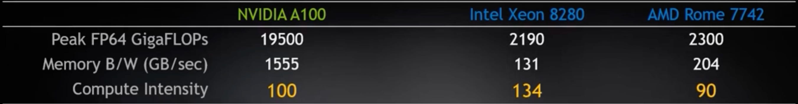
Ref: Comparison of compute intensities across current chips4
This is a comparison across a few modern chips (NVIDIA GPUs and Intel/AMD CPUs) regarding their peak operations per second and the bandwidth of their memory transfer. It's worth pointing out that A100 GPUs are significantly higher on both fronts largely because of their parallelization and memory proximity to their processing cores (see image below about the smaller and more abundant number of process units in a GPU vs CPU) and processor function with is designed primarily to do one operation, matrix multiplications, particularly well which can be made more efficient that the complex demands of multi-functional CPUs. The key metric, highlighted in yellow, is the relative ratio. The takeaway is that across these different architectures, in order to keep the processing unit busy (e.g., the FLOPs), the unit has to perform ~100 operations on every piece of FP64 precision data that the memory can serve up. If it does less, the processing unit is not used at full capacity. More importantly, this ratio has been getting worse over time. The image below is dated but the trend still holds:

Ref: A defining characteristic of computing is the continual separation between processing power and memory bandwidth which limits overall potential performance5
Ref: Highly recommended lecture on accelerated computing.
This is a particularly striking feature of the field -- and generally means that in most cases, the full power of a processing unit is left underutilized. The architecture of the GPU is designed to address this imbalance, in basic terms by adding more memory in smaller fractions and with a highly controlled hierarchy closer to the processing units (for example, a typical MacBook Pro may have 16GB of memory whereas a single H100 GPU may have 90GB in local high bandwidth memory alone) and by distributing the computing across a highly parallelized processor architecture, this type of architecture ensures that the memory queue of data is always full and can always serve the next open processor the moment that processor finishes. A high-level diagram looks like this;
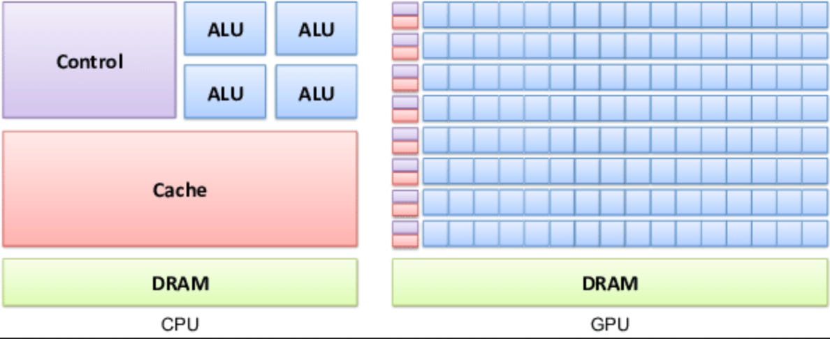
Ref: The design of CPU and GPUs are fundamentally different. The GPU distributes local cache memory and processing units in much smaller and more parallelized units that are specialized to do standard tasks. CPUs have more complex processing units that are designed to perform complex and diverse tasks. As cited from the video above a CPU is akin to cars on a highway, and a GPU is akin to a train. Both transport people but in distinct ways6
This architecture works particularly well when the operations that need to be performed can be run in a highly parallel way (e.g., have few, if any, dependencies). The origin of the GPU architectures was in rendering graphics for gaming -- which involves extensive linear transformations to project 3D images on a 2D screen at dynamic angles. These types of calculations are done with matrix multiplications, the same type of calculation that is at the center of most modern deep learning architectures. In a sense, the GPU and the transformer were the serendipitous match that pairs a gaming chip with the explosion of modern AI scaling.
Scaling Challenges
One of the features of the semiconductor industry is that a manufacturing install base of hundreds of billions of dollars of infrastructure exists to produce highly standardized chips from a form factor perspective. A standard silicon wafer is about 300mm in diameter and fits a few 100 or so chips on a single wafer -- the size of each chip is determined by the sizes of reticule which is the photolithographic light source for printing features. The size of chip features is determined by the wavelength of light and dimensions of photomasks, but the overall chip dimension is relatively standard-- they can just accommodate more features per chip. As the industry reaches some limitations on feature size, this presents limits on the number of features and memory that can be stored per chip. As the requirements for AI models, both training and inference, continue to increase, for example, for training and optimization approximately 14 bytes are required per model parameter, the challenges become more pronounced -- for example 90GB memory GPU might cap out training ~6-7B parameter model at FP32 precision. One approach that chip makers, such as NVIDIA, have taken to address this is to improve the connectivity between GPUs and to network multiple GPUs together in a way that can share common memory. Networking like NVLink has been a part of this solution and the more recent announcement of the B200 chip is a more integrated version that directly combines two individual chips together for a closer interface. A diagram of the Blackwell chip is below which is an integrated version of two individual reticules (the shape of a chip that would usually be cut up into individual chips from a single wafer.)

Ref: The Blackwell chip is basically just two chips fused togehter.7
The high bandwidth memory stacks are on the border of the chips which serve local memory to each GPU’s cache (which is considerably smaller at a few hundred MB on chip) and then to the processing units. One point of note from the NVIDIA lecture in the video above is that limits on this type of architecture are actually butting up against the speed of electricity in silicon -- quite an astounding fact.
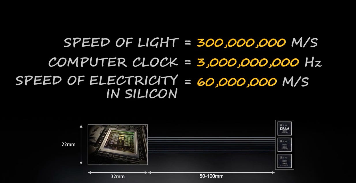
Ref: The competition of the speed of electrons in silicon with the physical distances required to travel is an extraordinary limitation of modern chip architecture that means that data can take several clock cycles just be more around between chips if they are physically separated (4).
Essentially what this means is that with increasingly fast processors that can perform increasing flops (operations per second), the physical chip architecture is actually running up against how far electrons can actually travel in a single clock cycle. The physical proximity of memory to the processing units and the connection bandwidth between them become limiting. This is an important distinction when considering NVIDIA's approach to scaling their systems like Blackwell by linking GPUs via NVLink. The approach has been marketed as representing a continuous shared memory space for up to 72 B200s or 144 equivalent GPUs, but their physical proximity is a factor -- perhaps up to a meter in end-to-end distance.
Breaking the Mold of Memory
The installed physical infrastructure for semiconductor manufacturing is probably not changing all that soon -- it is both expensive and extensive -- and designed to produce features on silicon of a specific size and shape. NVIDIA has taken the strategy of merging two chips together in a hybrid fashion but extending this strategy would consist of not cutting the wafer at all, but rather making one large chip with interconnects between at the sub-sections. This is the approach being taken by a company called Cerebras and can be seen in the image below. A specification comparison as provided by Cerebras is also below. Some of the key distinctions are in total memory of the high bandwidth variety, 1.2PB, vs 192GB for the B200, FLOPs which are 125 PFLOPs vs 4.4 for a single B200, and the "Fabric Bandwidth" which can be thought of as the processing flux of data across the chip. The large discrepancy here is due to the Cerebras chip’s large distributed local SRAM cache on the chip itself. Per their website, this is 44GB of local cache distributed across the chip compared a ~200MB for NVIDIA chips. This type of memory is more local and faster than high bandwidth memory (HBM) which Cerebras notes can make all 44GB of data 1 clock cycle away from a processor which NVIDIA has noted is a physical limitation of GPU architectures. The much larger value for the Cerebras chip is at least partially on account of just its physical size being bigger so there are more connection lanes You can see how the various interconnects including NVL (NVLink) can integrate multiple chips together increasing overall unit power, but they do not reach the memory throughput of the Cerebras chip.
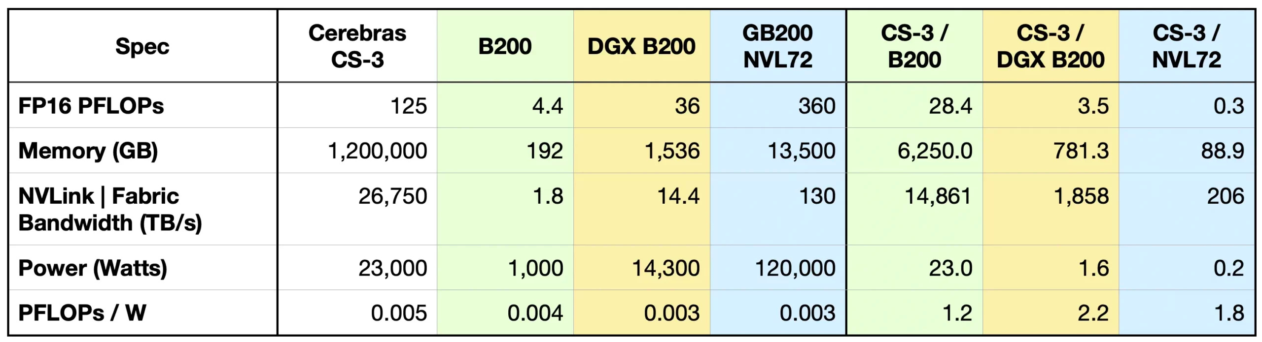
Ref: A comparison from Cerebras’ website shows some of the major differences between total memory capacity, FLOPs, fabric bandwidth between one large chip and even linked architectures of smaller GPU designs.8

Ref: Physical comparison of chips9
One Big Chip
The specifications of one single wafer scale chip are much larger than a single (or dual) GPU or any set of networked GPUs -- and this is largely just a physical property. A single chip has more transistors and more physical interface space for internal silicon-based interconnects vs. external connections like NVlink:
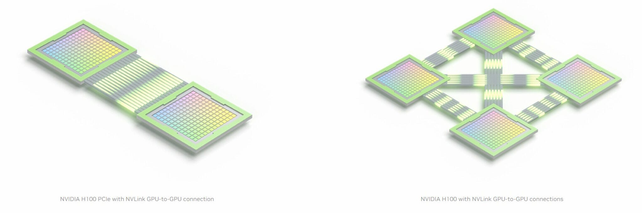
Ref: A simple diagram of NVLink connecting multiple GPUs. This linking system can be expanded across up to ~144 effective GPUs (72 Blackwell chips)10
and is manufactured on the same substrate which has consistent properties across the chip, for example, under thermal expansion, which is important for keeping feature alignment when the chip heats up. A downside of a single wafer chip is that manufacturing is never perfect and single chips are often discarded if they don't meet specifications, but this cannot be done with a wafer scale chip so the logic to reroute around defective single chips is important for keeping the whole wafer working.
The net-net of this single wafer is that it's probably just faster because all of its features are on the same silicon substrate, its memory and processors can be optimally distributed across a larger area and its interface area with other chips for attached memory is also just physically larger. By distributing memory and processing units continuously and optimally across a larger surface area, the limitations of memory bandwidth/processing speed/speed of electricity in silicon can be more flexibly matched.
Optimizing Speed for Inference
Another dimension of AI performance is perhaps less concerned with absolute memory and more concerned with raw speed. Chip design on this end is focused on the physical design of a single chip to optimize a specific type of processing architecture. GPUs have done this for graphics (which are quite similar to the matrix multiplication for many AI models), but this can be thought of as pushing those bounds even further. Companies like Groq and Etched are designing architecture/application specific chip architectures, for example for the transformer architecture, to optimize inference speeds. The design of these chips looks highly "structural" with Groq having what they call "superlanes" feeding memory to matrix multiplication blocks (MXM). There is currently a token per second war going on in the inference space with Groq seemingly leading the way:
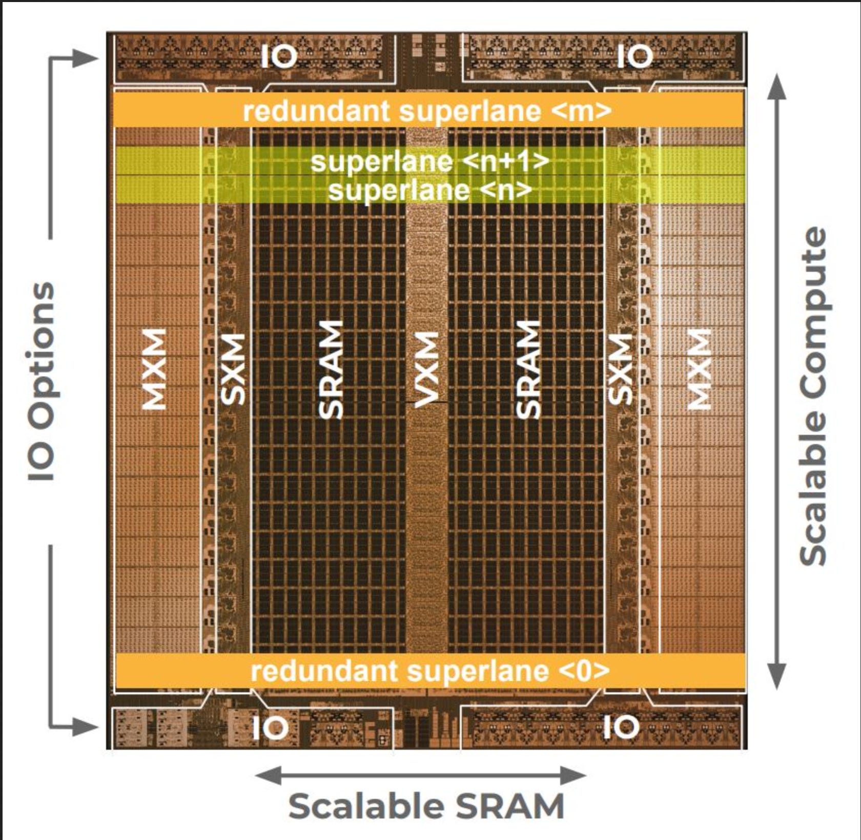
Ref: The Groq chip is designed for optimal physical architecture to run matrix multiplications.11
Per Groq's materials, the output of this design is vastly improved tokens/second compared to any provider using GPUs.
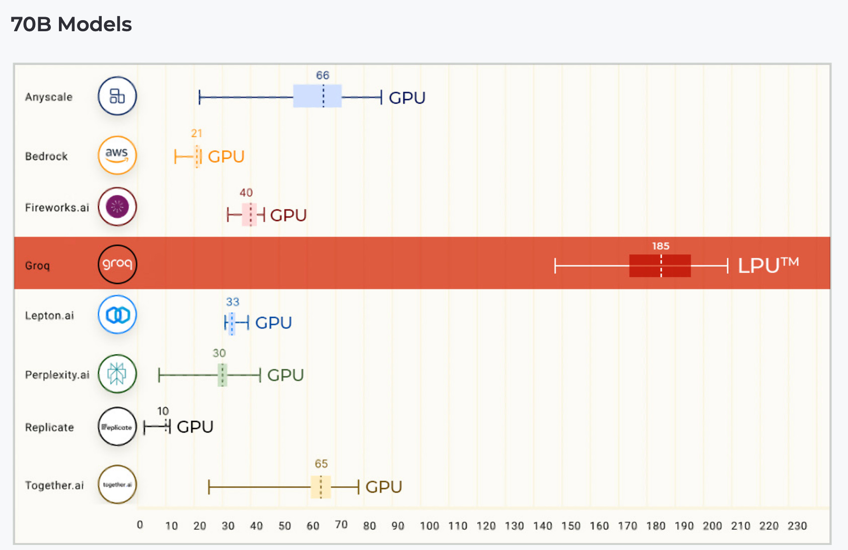
Ref: Model serving in tokens per second. Groq has been cited as requiring relatively large infrastructure to achieve this which may not be practical for local use, but for model serving and cloud hosting, can be very fast. 12
Fragmenting Use Cases
The landscape of use cases and optimal chip architectures for AI is fragmenting. A few of the important trends are below:
Frontier models will get bigger in terms of parameters and compute. Up until the release of the o1 model from OpenAI, the race to scale parameter count was intense, with the largest growing to over 1T parameters in total. The introduction of o1 has shifted this focus a bit away from raw parameter scale but, this trend will still likely continue. Frontier research in the mathematics of the properties of infinite random matrices and infinite depth neural networks is active at places like xAI13 and we should expect that this trend will continue.
Practical models will get smaller in terms of parameters. *smaller* is relative -- probably better phrased as they will grow slower in parameter count and the pressure will be to reduce parameter count. The practical use case of this will be fine-tuning smaller models on data generated from larger models to make them use-case performant. An example of this from a talk from OpenPipe is below:
It is possible to take a more sophisticated model, in this case, the Claude Sonnet 3.5 Mixture of Agents model which is expensive, and train smaller models on the output to obtain a similar performance at a much lower cost per token.
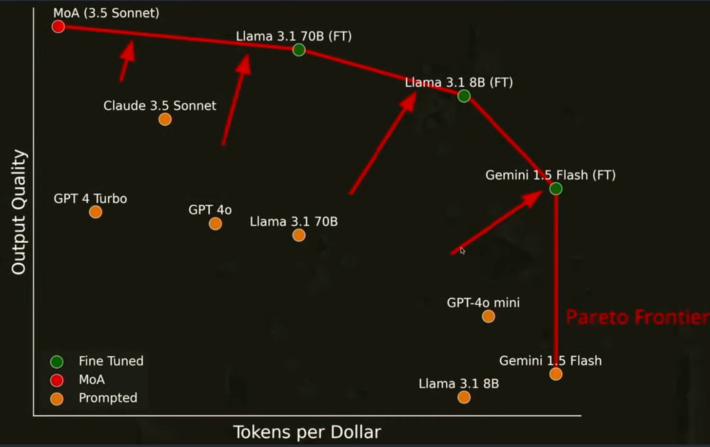
Ref: Fine-tuning smaller models on the outputs of larger and more performant ones is demonstrated to substantially increase the domain utility of small models potentially reaching similar output quality as large models at substantially lower cost for specific use cases14
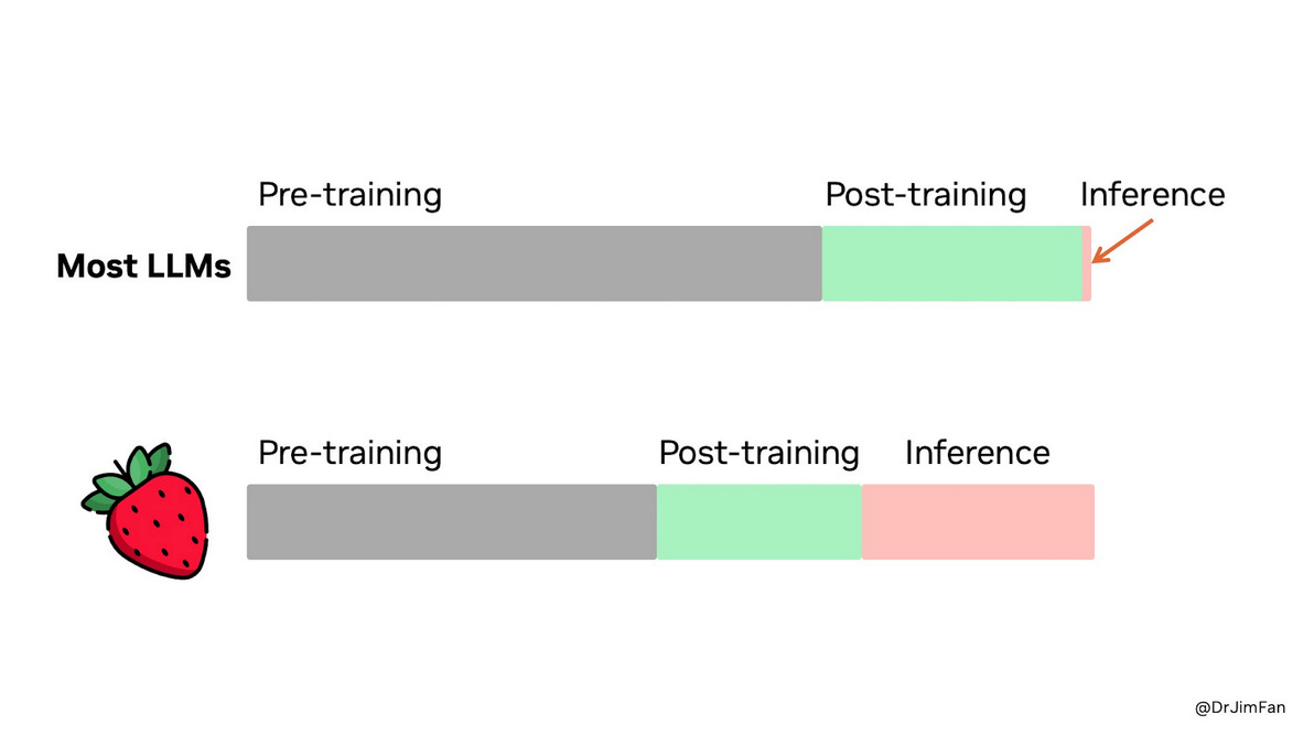
Inference speed in tokens per second will be increasingly important, particularly for a new class of "reasoning" models, multi-agent models, and real-world use cases like speech2speech. For many, the interface with LLMs is via a chatbot and the impression is that the speed of the response should be comparable to the speed of human consumption, but this is changing dramatically. Increasingly, the consumers of generative AI are other computers or models, and their speed of consumption is vastly greater. There's no practical rate limiting factor to how fast this should or could be and, in general, the faster the inference speed, the more capable many models can become (even if inference speed is for internally generated "thinking" tokens). This shifts the balance of where the compute should reside. A cartoon from Jim Fan at NVIDIA shows this:

Ref: The o1 family of models (strawberry) is a new class of models that trades off computation at the time of inference for pretraining. Essentially they “think” about their answers. This has been likened to System 1 and System 2 thinking popularized by Kahneman15. More about this can be read here16

Jensen's Inequality
This is a play on words; however, it has some basis. When looking at the diverse space of computing requirements for the expanding of AI applications it's an interesting case study to assess where different providers land -- at least technologically. NVIDIA is by far the dominant player, but it's not evident that their GPU chip architecture is the best architecture for the fragmenting use cases -- and from a historical perspective, it doesn’t seem particularly designed to be so. The RAM requirements of gaming did not approach the requirements of trillion parameter deep neural networks, and the computing model of transformers (or other architectures), despite being in principle a matrix multiplication, seems a serendipitous coincidence for the GPU architecture, not an express design.
It seems then, that the GPU is a high-performance multipurpose architecture that can be used across settings, but may not be optimal, at least from a technology perspective, for the growing segments of AI use cases. The approaches to merge chip dies, improve inter-GPU memory connections, and so forth are all efforts to expand optimizations, but not fundamentally change, a core architecture.
Jensen's inequality17 is a mathematical concept that states that for a convex function, the value of the function assessed at the expected value of an input distribution is always less than the expected value of the function assessed across that input distribution.
In analogous terms, one way to think about this is that in a world of increasing value from specialization, a generalist approach will be sub-optimal for any specific use case.
It is somewhat strange to say that GPUs may now be considered a generalist computing architecture, but it is and will continue to be the case in the rapidly advancing space of AI compute requirements.
The history of semiconductors in computing is a litany of case studies in rapid technological progress and rapid commoditization. Accelerated computing will be no different. Early technology advantages are likely to rapidly erode, and commercial prowess will carry the day more consistently in the long term. NVIDIA has certainly embraced Andy Grove’s “only the paranoid survive" and rightfully so by taking their near-term dominance and expanding their market applications into durable application-oriented goods and services like cloud hosting/serving, robotics, and early ventures into drug discovery and healthcare. NVIDIA will likely need to reinvent itself over time in the wake of technological innovation in the chip space that is rapidly approaching bottlenecks by the laws of physics as well as increasing specialization of computing and application requirements. They certainly have the resources to do so.
It's an amazing time to be alive.
Additional Reading
In addition to the references, the following is a useful article on this topic
https://towardsdatascience.com/groq-intuitively-and-exhaustively-explained-01e3fcd727ab
References
https://www.reuters.com/technology/microsoft-openai-planning-100-billion-data-center-project-information-reports-2024-03-29/
https://arstechnica.com/tech-policy/2024/09/openai-asked-us-to-approve-energy-guzzling-5gw-data-centers-report-says/
https://semiengineering.com/wp-content/uploads/2018/09/Screen-Shot-2017-04-26-at-1.08.57-PM.png
www.youtube.com/watch?v=3l10o0DYJXg
https://www.forrestthewoods.com/blog/memory-bandwidth-napkin-math/assets/img/01.png
https://www.researchgate.net/profile/Ahcene-Bounceur/publication/308730753/figure/fig1/AS:614044658573321@1523411063058/Difference-Between-GPU-and-CPU-Architecture-GPU-architecture-belongs-to-the-family-of.png
https://i.pcmag.com/imagery/articles/05sVvCWIsXR56ECNZzbfwDT-3..v1710781011.png
https://cerebras.ai/blog/cerebras-cs-3-vs-nvidia-b200-2024-ai-accelerators-compared
https://cdn.wccftech.com/wp-content/uploads/2019/08/cerebras-wse-nvidia-v100-featured-image.jpg
https://blogs.nvidia.com/wp-content/uploads/2023/03/NVLink-types-scaled.jpg
https://www.eetimes.com/wp-content/uploads/Groq-Chip-Layout.jpg
https://groq.com/wp-content/uploads/2024/05/2024_GroqThoughts_Inference-Speed-Is-the-Key-To-Unleashing-AIs-Potential.pdf?hss_channel=lcp-12994410
https://paperswithcode.com/paper/tensor-programs-vi-feature-learning-in
www.youtube.com/watch?v=dYhR2k3rHQU0)
https://analyticsindiamag.com/ai-origins-evolution/sambanova-cerebras-and-groq-clash-over-token-speed-in-wake-of-openai-o1-launch/

https://en.wikipedia.org/wiki/Jensen%27s_inequality
Header image reference: https://ppss.kr/wp-content/uploads/2014/10/Generalist-Specialist.jpg